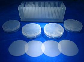
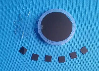
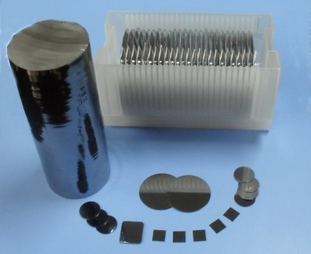
Silicon Wafers - Silicon wafers can be used in the production and deep processing of diodes, rectifier devices, circuits, and solar cell products. Its subsequent product integrated circuits and semiconductor separation devices have been widely used in various fields, and also occupy an important position in military electronic equipment.
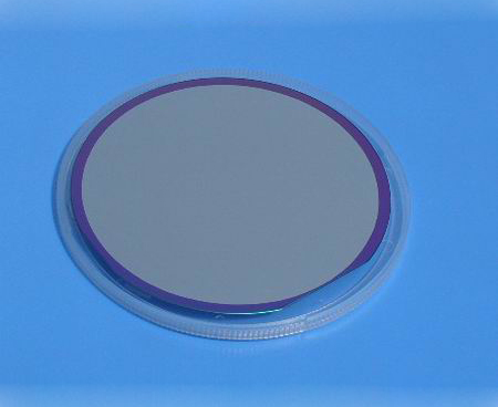
Thermal oxide Silicon wafers - The Thermal oxide Silicon wafer is growth an oxide layer(SiO2) on Silicon wafer, also known as "SiO2 + Si wafer". Growth of a good quality oxide layer on the surface of Silicon wafer is important to the entire semiconductor integrated circuit fabrication process.
SOI Wafers - Silicon-On-Insulator wafer (SOI) which is silicon on an insulating substrate (Si + SiO2 + Si), and a buried oxide layer is introduced between the top silicon and the back substrate.
Sapphire Wafers - Sapphire crystal has good thermal properties, excellent electrical properties and dielectric properties. Sapphire, Al2O3 are widely used in industrial, defence and scientific research (such as high-temperature infrared windows, etc.).
Germanium wafers - Germanium(Ge) single crystal is an important semiconductor material that can be used to fabricate semiconductor devices, infrared optics, and solar cell substrates.