
 UK
 Europe
 Netherlands
The Materials Behind the Next Generation of Electronics
The electronics industry is developing new types of electronic devices for applications including AI hardware, advanced semiconductor packaging, flexible electronics and wearable devices. These developments are also driving research into new semiconductor materials, thin films and deposition methods.
Silicon remains central to electronics but it is now used alongside a wider range of materials. Gallium nitride (GaN), silicon carbide (SiC) and oxide semiconductors such as indium gallium zinc oxide (IGZO) are being used and studied for different applications.
The most suitable material depends on the device, substrate and manufacturing process.
New Materials for Semiconductor Applications
Silicon is still the most widely used semiconductor material, but other materials offer properties suited to specific applications.
GaN and SiC are wide-bandgap semiconductor materials used in power electronics and high frequency applications. They can operate at higher voltages and temperatures than traditional silicon, making them useful in a range of applications.
Oxide semiconductors are another area of research. Indium gallium zinc oxide (IGZO) is widely used in thin-film transistors for display applications and is also being investigated for flexible and emerging electronics.
A review published in Materials Science in Semiconductor Processing in August 2026 examined developments in thin-film transistors, focusing on flexible electronics, wearable devices and brain-like neuromorphic systems. This reflects the ongoing research into materials and processing methods for different electronic applications.
Research published earlier in 2026 has also examined how changing the composition of oxide semiconductor films can affect their electrical and optical properties. These studies demonstrate how material composition and processing methods can be adjusted to meet different application requirements.
Testbourne supplies high-purity elemental and compound materials in forms including sputtering targets and evaporation materials. Its electronics range includes materials for PVD thin films, capacitors, resistors and semiconductor applications.
For specialist projects, sourcing a material that meets the required specification can also be an important consideration. Testbourne draws on 40 years of experience and an established network within the materials industry to support customers with specialist material requirements.
Advanced Packaging and 3D Electronics
The rapid development of AI hardware is also increasing demand for advanced semiconductor packaging. Applied Materials said in August 2026 that it expects its advanced-packaging revenue to grow by more than 70% during the year, up from its previous forecast of more than 50%. The company linked this increase to continued investment in AI infrastructure.
High-bandwidth memory (HBM) uses stacked memory components to support high data-transfer rates. Chiplets and other advanced packaging methods allow multiple components to be integrated within a single package.
These approaches create new manufacturing requirements, including the deposition of thin films across different surfaces and structures. The deposition process depends on the material, structure and film required.
Physical Vapour Deposition (PVD) is one method used to deposit thin films. During sputtering, ions strike a solid target and eject material that forms a film on a substrate.
Testbourne supplies sputtering targets in metals, alloys and compounds, with different sizes and configurations available for different systems.
Flexible and Wearable Electronics
Flexible electronics create different material and processing requirements.
Flexible displays, wearable sensors and other devices can use polymer or other temperature-sensitive substrates. Researchers are therefore investigating ways to deposit electronic layers without exceeding the temperature limits of these materials.
The Materials Science in Semiconductor Processing review of thin-film transistors also identifies low-temperature manufacturing as a key breakthrough for flexible electronics.
Atomic Layer Deposition (ALD) and Physical Vapour Deposition (PVD) are different deposition methods and the choice depends on the material and application. Testbourne supports PVD applications through its sputtering targets and evaporation materials, including metals, alloys and compounds.
Why Material Specification Matters
As electronic devices and thin-film structures become more specialised, the material needs to meet the requirements of the application.
Purity is one consideration. Composition, physical form, dimensions and compatibility with the deposition process can also affect material selection.
For sputtering, the target needs to be suitable for the deposition system and the required film.
Target bonding can also be important for some sputtering applications. Testbourne provides indium-based metallic bonding and elastomer bonding, depending on the target and process requirements.
For customers working with specialist materials, continuity of supply can also be an important consideration. Testbourne can support customers looking for local sourcing options, drawing on its established materials network and industry experience.
Supporting Research into Emerging Electronics
Developments in AI hardware, advanced packaging, flexible electronics and semiconductor devices are creating new areas of materials research.
The materials used in these applications vary according to the device and manufacturing process. A material used for a thin-film transistor may have different requirements from one used in a power semiconductor or an advanced packaging process.
Testbourne supplies high-purity materials, sputtering targets, evaporation materials, single crystals, foils, wires and other scientific materials for research and industrial applications. Its electronics offering includes materials for PVD thin films, capacitors, resistors, semiconductors and integrated circuits.
Alongside supplying specialist materials, Testbourne can support customers with material sourcing and refining requirements. Its 40 years of experience and network within the materials industry provide a long-standing base for supporting customers with specialist requirements and security of supply.
For research teams developing new electronic materials and thin-film processes, access to the appropriate material composition, purity and form is an important part of the development process.
Related

Your Partner in Collaboration, Innovation and Reliability
03 Feb 2025If you’re looking for a partner who understands the intricate needs of R&D and offers more than just products, Testbourne is the name to trust.
How to Source High Purity Materials with Testbourne
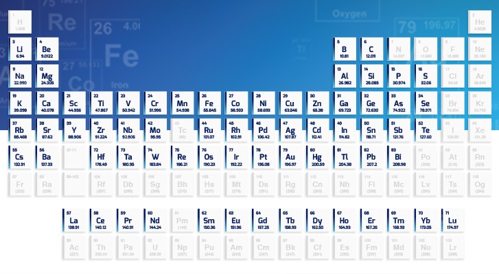
26 Aug 2025Quickly find high-purity materials by element with Testbourne’s interactive periodic table. Explore forms, specs and get expert support.